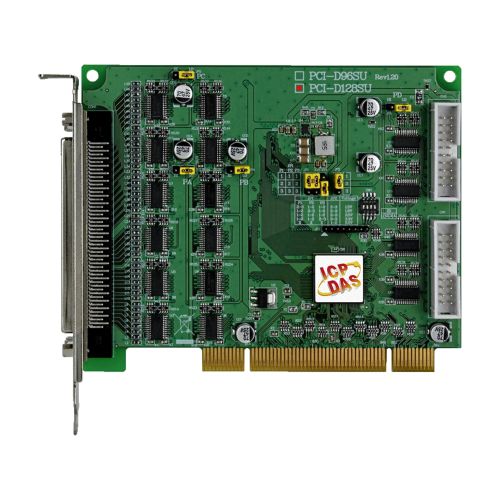
PCI-D128SU CR
Universal PCI, 128-ch, 32-bit Digital I/O Board
Free Shipping
Features
- Support the +3.3/+5 V PCI bus
- 128 Channels of Digital I/O
- Four 32-bit Bi-direction I/O Ports
- Digital Pattern Generator
- Bi-direction Programmable I/O Ports under Software Control
- Pattern-matching and Change State Interrupt Monitoring
- DIO Operating Voltage: +1.8 V, +2.5 V, +3.3 V, +5 V
- Pull-high/Pull-low Jumpers for DI Channels
- Supports Card ID (SMD Switch)
- Supports a High-density SCSI II 100-pin Connector
Introduction
The PCI-D128SU supports 3.3 V/5 V PCI bus. These cards provide 128 Digital I/O lines that consist of four 32-bit bi-directional ports for use in a variety of Digital I/O applications. Each channel could be setting for DI or Output. They provide a variety of operating voltage (+1.8 V, +2.5 V, +3.3 V and +5 V) for customers need.
The PCI-D128SU cards include an onboard Card ID switch that enables the board to be recognized via software if two or more boards are installed in the same computer. The pull-high/low jumpers allow the DI status to be predefined instead of remaining floating if the DI channels are disconnected or interrupted. The PCI-D96SU provides a single high-density connector that reduces the amount of installation space required for the card in the computer.
These cards support various OS versions, such as DOS and 32/64-bit Windows 10/8/7/2008/2003/XP. DLL and Active X control together with various language sample programs based on Turbo C++, Borland C++, Microsoft C++, Visual C++, Borland Delphi, Borland C++ Builder, Visual Basic, C#.NET, Visual Basic.NET and LabVIEW are provided in order to help users quickly and easily develop their own applications.
Specifications
Hardware
Card ID: Yes (4-bit)
Connector: Female SCSI II 100-pin x 1
20-pin Box Header x 2
Digital Input
Channels: 128 (Bi-Direction)
Type: 1.8 V/TTL, 2.5 V/TTL , 3.3 V/TTL, 5 V/TTL
ON Voltage Level: 1.8V/TTL(Logic 1: 1.2 V Min.)
2.5V/TTL(Logic 1: 1.7 V Min.)
3.3V/TTL(Logic 1: 2.0 V Min.)
5V/TTL(Logic 1: 3.5 V Min.)
OFF Voltage Level: 1.8V/TTL(Logic 0: 0.65 V Max.)
2.5V/TTL(Logic 0: 0.7 V Max.)
3.3V/TTL(Logic 0: 0.8 V Max.)
5V/TTL(Logic 0: 1.5 V Max.)
Response Speed: 1 MHz (Typical)
Trigger Mode: Software (Pattern Match, Change of Status)
Data Transfer: Polling, Interrupt
Digital Output
Channels: 128 (Bi-Direction)
Type: 1.8 V/TTL, 2.5 V/TTL , 3.3 V/TTL, 5 V/TTL
Sink/Source (NPN/PNP): Sink: 6 mA @ 0.33 V
Source: 6 mA @ 4.77 V
Operation Mode: Static update, Waveform generation
Load Voltage: 1.8V/TTL(Logic 0: 0.65 V Max. ,Logic 1: 1.2 V Min.)
2.5V/TTL(Logic 0: 0.7 V Max. ,Logic 1: 1.7 V Min.)
3.3V/TTL(Logic 0: 0.8 V Max. ,Logic 1: 2.0 V Min.)
5V/TTL(Logic 0: 1.5 V Max. ,Logic 1: 3.5 V Min.)
Response Speed: 1 MHz (Typical)
PC Bus
Type: 3.3 V/5 V Universal PCI, 32-bit, 33 MHz
Data Bus: 32-bit
Power
Consumption: 760 mA @ +5 V
Mechanical
Dimensions (mm): 105 x 129 x 22 (W x L x D)
Environment
Operating Temperature: 0 ~ +60°C
Storage Temperature: -20 ~ +70°C
Humidity: 5 ~ 85% RH, Non-condensing


